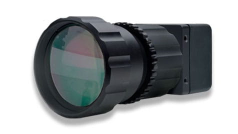
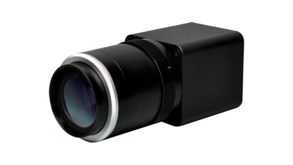
1280JSX HD Camera
1280 x 1024 @ 12.5µm, high definition, high sensitivity and mil-rugged
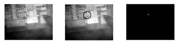
Photon counting APD modules and photon emission microscopy with InGaAs image sensors are used with Focused Ion Beam (FIB) systems to locate faults in integrated circuits. Once the fault has been located, the circuit is modified to eliminate the problem, thereby improving throughput and efficiency of failure analysis. The cooled InGaAs focal plane array (FPA) provides the sensitivity to "see" the faint emissions from the faulty transistor or overloaded node. The SWIR camera can see these emissions through the integrated circuit (IC) substrate, viewing the circuit layers through the backside of the device, or the front side if the top-side interconnect circuitry does not block the view.
In the images below, a short wave infrared array can detect the faint emission given off by the faulty silicon circuit, improving the quality.
Outside of the FIB vacuum systems, room temperature InGaAs area cameras mounted on microscopes with SWIR optics and illumination are used for examining circuit layers on integrated circuit wafers or device die to verify the circuit layout. This helps the circuit designer identify a problem circuit and decide the best modification strategy. After the modification, the physical changes can also be inspected with the SWIR cameras. Nano structures in Micro-Electro-Mechanical Systems also benefit from inspection with SWIR cameras. For large silicon wafer ICs or MEMS wafers, InGaAs line scan cameras, mounted on microscopes with motorized stages can be used for maximum resolution.
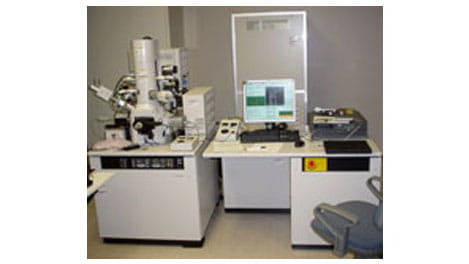
The image below is an example of FIB hardware work station for integrated circuit inspection and modification.