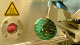
A wafer during the glass film deposition process.
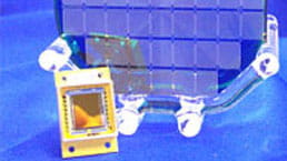
The device fabrication process starts by growing a thin crystalline layer of semiconducting Indium Gallium Arsenide (InGaAs) on an Indium Phosphide (InP) substrate wafer. The InGaAs material absorbs light in the NIR spectrum and acts as a highly efficient optical detector material in this wavelength band. Next, we apply a thin layer of insulating glass. This glass layer protects the wafer surface and provides electrical isolation between the various picture elements (pixels) in the array. Then, tiny holes – less than 1/5 the thickness of a human hair – are opened through the thin glass layer using a special technique called photolithography. Certain materials & metals are added to the crystal in each of these holes to form the pixel electrodes. Next, the wafers are diced into chips, each chip an imaging array containing thousands of pixels. Each imaging chip is approximately the size of a dime.
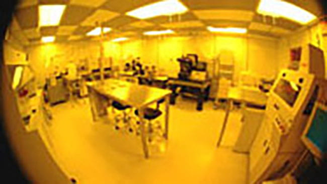
Since even the smallest of dust particles can ruin pixels in the NIR imager, all these critical fabrication processes take place in a special cleanroom environment. Highly trained technicians perform these critical tasks wearing special garments designed to minimize contaminant generation. This cleanroom environment contains 1000 times fewer particles than the typical clean air you breathe.
The InGaAs pixel array chips are carefully inspected and tested to meet electrical and optical performance specifications before being connected to a Read-Out Integrated Circuit (ROIC) chip. The ROICs are also designed at SUI to provide for a broad range of camera functionality. The InGaAs pixel array/ROIC assembly is then sealed within a dry, temperature-controlled package behind a glass window to create a packaged assembly. The packaged assembly can then be integrated into a camera with optics, software and other attachments that will produce a flawless image of the NIR/SWIR spectrum.
Finished Sensors Unlimited products, all using InGaAs pixel chips in various forms, include 2D NIR/SWIR cameras, NIR/SWIR linear arrays and avalanche photodiodes (APDs). These products are widely used in surveillance, night-vision devices, industrial machine vision, process control, laser beam profiling, scientific instrumentation and medical imaging. The latest development is the world's smallest NIR/SWIR camera.
One key to our success is full in-house production and control of every step in the InGaAs process, from crystal growth to finished camera. Sensors Unlimited is a leader in funded R&D to advance the technology of NIR/SWIR imaging.