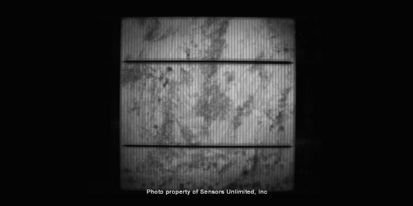
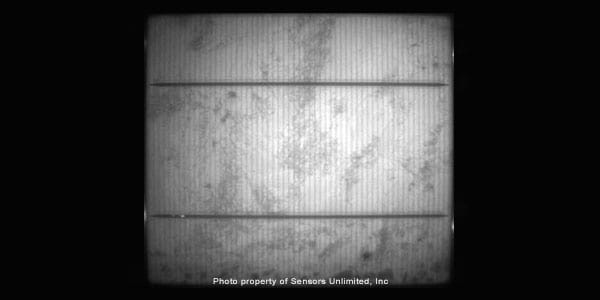
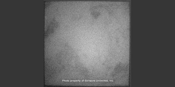
Figure 1a:
SWIR PL image of a finished cell acquired with on lnGaAs area photodiode array using a 16-ms exposure time, at the rate of 60 frames/second. The InGaAs camera resolution is 320 x 240 pixels.
NIR Trends: Photoluminescence Inspection of Photovoltaics with SWIR Imaging
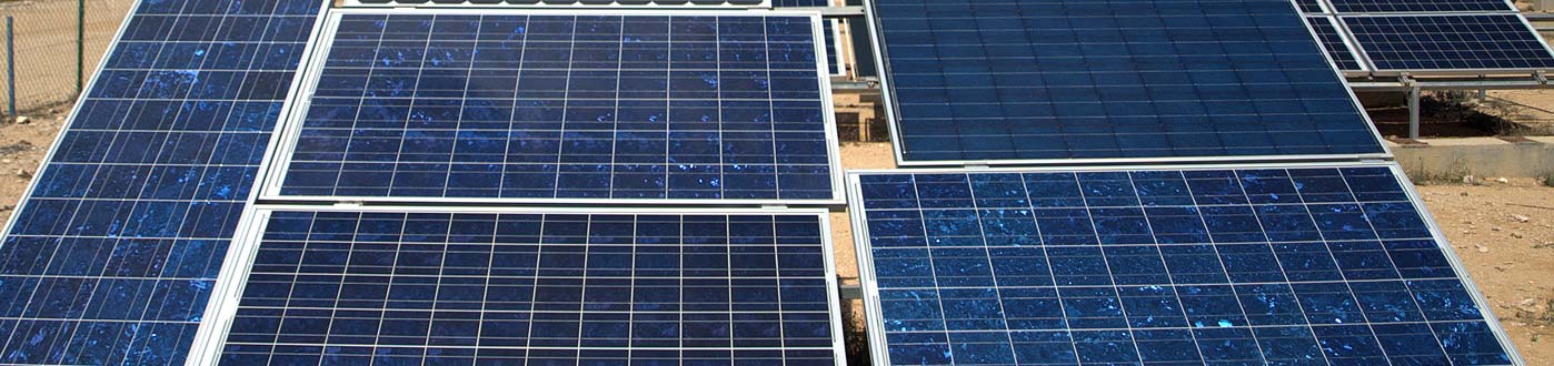
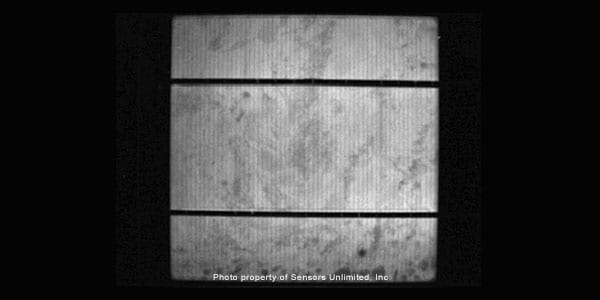
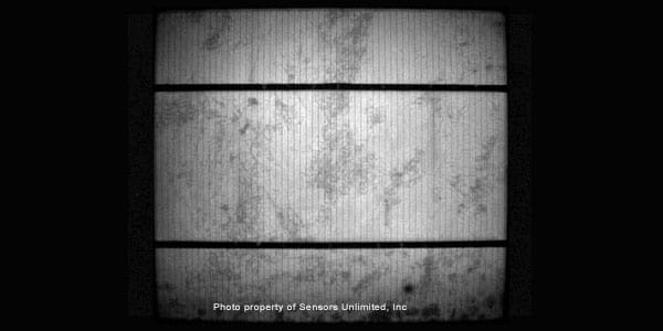
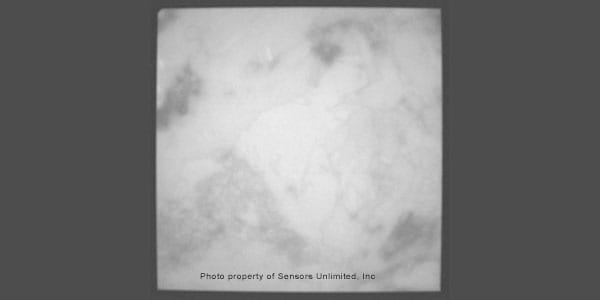
Contactless machine-vision inspection using photoluminescence (PL) imaging with shortwave infrared (SWIR) cameras can help solar cell producers improve both efficiency and quality of their photovoltaic products. Inspection of silicon bulk ingots, sliced wafers, processed layers, and complete photovoltaic cells is possible with SWIR imaging. The PL emissions occur at the wavelengths associated with the semiconductor bandgap, which are visible to high-sensitivity, uncooled, indium gallium arsenide (InGaAs) cameras, even while imaging at video frame rates. This inspection technique illuminates the objects of interest with high optical power at one wavelength, and photons are absorbed in the bulk material. Some energy is lost as heat in the interaction with the molecular structure and the remaining energy causes a photon to be re-emitted at a longer wavelength. The uniformity and intensity of the resulting glow is sensitive to many parameters of the material, and of subsequent processing steps. In many cases, properties of the material, such as minority carrier lifetime, can be mapped from the PL image, and these maps will directly relate to how well the final product will perform as a solar cell.
The PL images were acquired with illumination provided by four semiconductor diode lasers at 810 nm with overlapping diffused beams to achieve uniform illumination, one source per side. Approximately 30 W of illumination was used for Figures 1 and 3 of the L images shown, 60 W for Figure 4. The images were taken at different times using the same 16 mm f/1.8 lens, with the 810 nm excitation filtered at the lens by RG-1000 long pass filters (the cut-on wavelength was 1000 nm); one filter was used with the InGaAs camera, there were stacked when used with the silicon camera. The test station, silicon camera images and wafers were provided by the National Renewable Energy Labs (NREL) at Golden, CO.
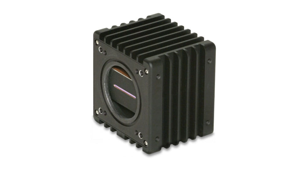
Both Sensors Unlimited linescan and area cameras can be used for photoluminescence inspection of photovoltaic solar cells. For more information on this subject click here.
As seen in the 11/18/09 edition of the Photonics Online (www.photonicsonline.com) newsletter.